Backside Power Delivery Network Integration in Physical Design
Three rival foundry approaches reshape chip design at the physical layout stage.
Backside power delivery moves a chip's power rails off the front of the wafer and onto the back, handing signal wires the entire frontside metal stack to themselves. That single relocation forces changes at every stage of physical design, from how a floorplan gets drawn on day one to how an IR-drop signoff report gets read months later. Anyone treating this as an incremental process tweak is underestimating it: BSPDN rewrites assumptions about chip layout that have held since multi-layer copper interconnect became standard, and the foundries have not converged on a single way to build it. That disagreement, not the concept itself, is where the real engineering risk sits.
What BSPDN is and how its key building blocks work together
Every advanced node has fought the same losing battle. More transistors and more metal layers mean a longer, more resistive path between the power supply and the device that needs the current. At sub-5nm nodes, frontside power delivery loses roughly 10% of supply voltage just crossing the copper BEOL layers, and that loss gets worse as layer counts climb past ten, sometimes past twenty. Power and signal wiring also fight for the same real estate: power rails alone eat up something like 20% of frontside routing resources, and at 3nm and below that overlap hardens into routing congestion, worse IR drop, and noise coupling between power and signal nets that designers used to shrug off.
Backside power delivery network design answers this by moving VDD and VSS off the front of the die completely. The rails go to the wafer's backside, and power and signal stop competing for the same layers.
Three building blocks make this work, and they depend on each other in sequence. Buried Power Rails (BPRs) sit below the transistor fins, partly inside the silicon substrate and partly inside the shallow trench isolation oxide. They were proposed specifically to let scaling continue past 5nm, and because they're physically thicker than a frontside metal track, they carry current with lower resistance without eating into the BEOL layers signal wires need. Nano-through-silicon vias (nTSVs) connect the backside power network up to those buried rails, and a 2025 research result puts hard numbers on how demanding that step is: wafers thinned to a final silicon thickness of 500 nanometers, total thickness variation held under 15 nanometers, alignment accuracy tighter than 10 nanometers. A conventional through-silicon via runs about 10 micrometers in diameter; an nTSV is roughly 100 nanometers, two orders of magnitude smaller. The third block is the backside metal layer itself, built far thicker than any frontside signal layer. This is where BSPDN gets its lower resistance and higher current-carrying capacity.
Getting there takes a specific manufacturing sequence: SiCN-to-SiCN dielectric fusion bonding, a post-bond anneal, then thinning the wafer from around 775 micrometers down to a SiGe etch-stop layer. Intel's version, PowerVia, forms backside contacts early in the process flow, alongside the n- and p-type transistors, using either copper or lower-resistance ruthenium for the via fill. A late-2025 result demonstrated a ruthenium nTSV array with an aspect ratio of 10.4-to-1, reached through a multi-step etch process. That number is the tell: etch technology still has real distance to cover before this is manufacturable at volume.
The three foundry architectures and what distinguishes them
Every major foundry has bought into BSPDN as a direction. None of them agree on where the backside contact should land, and that disagreement is not a minor implementation detail. It decides how complex the process is to build, how much area scaling a design can actually claim, and what a physical design team inherits when the process design kit lands on their desk.
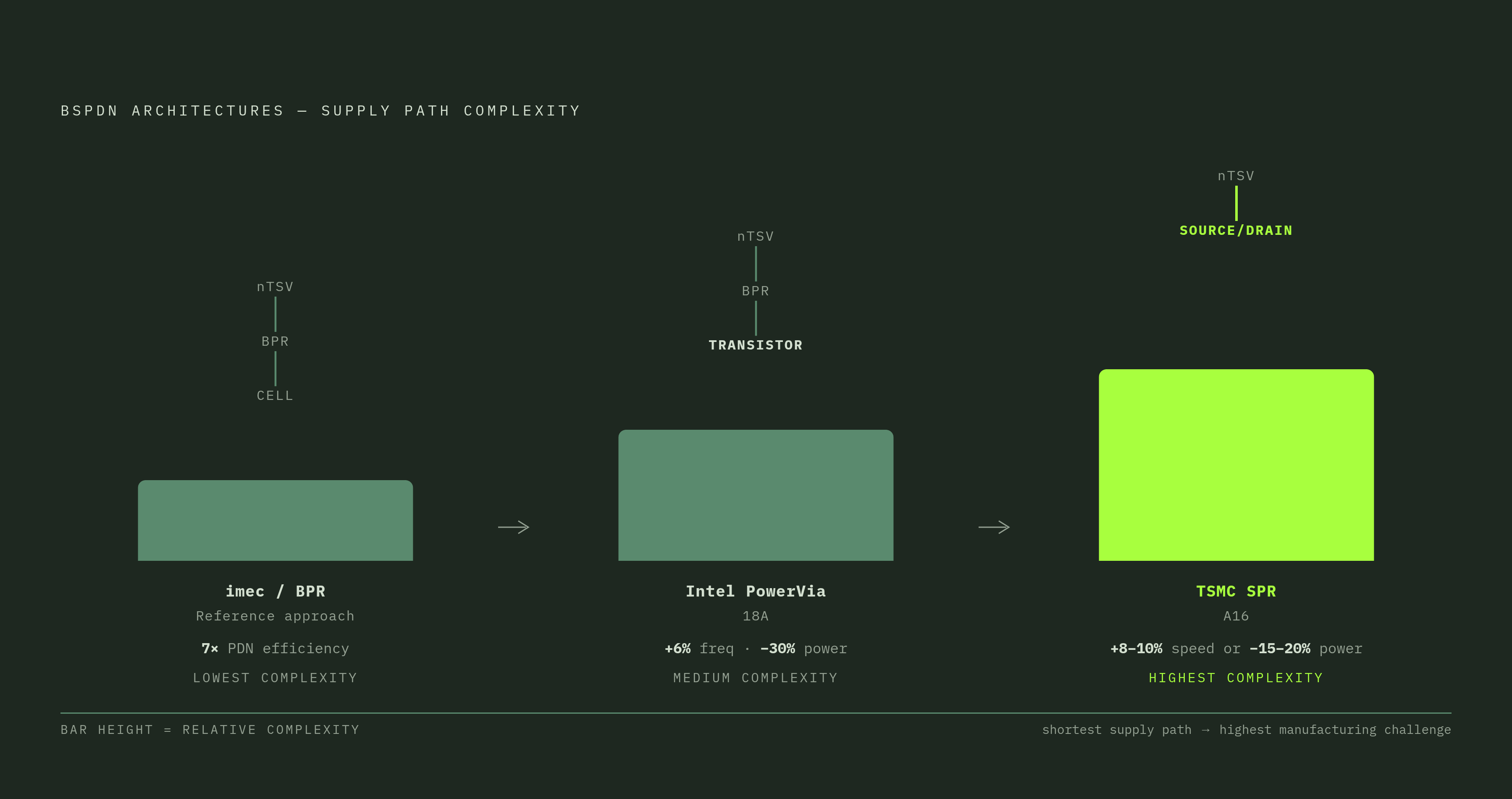
imec's Buried Power Rail approach connects backside power to the BPR of each logic cell through nTSVs. It's the oldest of the three techniques and the one that validated the whole concept: early simulations showed a backside PDN running seven times more efficiently than a traditional frontside PDN. It also carries the least production complexity of the three, which is part of why it became the benchmark everyone else gets measured against.
Intel's PowerVia, shipping in 18A, connects power to the cell or transistor contact through nTSVs that land on BPRs, a complexity level between imec's approach and TSMC's. Intel proved this out with the Blue Sky Creek test chip, which hit over 90% cell utilization against traditional frontside PDN designs that top out around 75 to 80%. 18A pairs PowerVia with RibbonFET gate-all-around transistors, and Panther Lake CPUs are the first volume product on the node. Silicon-validated SRAM results show a 0.021 square-micrometer cell at 38.1 megabits per square millimeter array density, a shipped number.
TSMC's Super Power Rail, arriving in A16, skips the intermediate BPR step and connects the backside network directly to each transistor's source and drain. That's the shortest possible path from supply to device, which is why it carries the highest scaling potential of the three. It's also the most complex and expensive BSPDN process TSMC has discussed, harder to build than PowerVia, and that difficulty is almost certainly why TSMC pushed the architecture back from N2P to A16 instead of shipping it sooner. Rushing Super Power Rail into N2P would have meant shipping a yield problem.
Samsung's plans center on SF2Z, a variant of its 2-nanometer SF2/2GAP process, with BSPDN reserved for that node rather than the base SF2 process. ARM test chips with buried power delivery have already shown a 19% die shrink, with mass production targeted for 2027. Samsung's 1.4-nanometer roadmap calls for buried power delivery too, extending the same bet further out.
None of these choices stays theoretical once it reaches a physical design team. Where the backside contact lands decides what changes in the cell library, how IR-drop analysis gets structured, and what signoff criteria apply downstream. TSMC says A16's Super Power Rail preserves N2P's gate density and its NanoFlex design flexibility, keeping the ability for design teams to tune cell layouts for performance, power, and area instead of getting locked into one rigid template. That detail matters more once the standard-cell conversation starts.
The quantified PPA case and what the numbers mean for design targets
IBM Research offers the most credible independent quantification of what BSPDN buys a design, and the range is wide enough to serve as a planning target rather than a marketing line: IR drop falls by 20 to 30%, maximum frequency rises by 2 to 6%, core area shrinks by 5 to 15%, and utilization clears 90%.
Foundry-reported numbers point the same direction, though they aren't directly comparable to one another, since each is measured on a different test vehicle under different conditions. Intel's Blue Sky Creek chip showed a 6% frequency gain alongside a 30% reduction in power loss. TSMC claims A16 delivers 8 to 10% higher speed at the same power as N2P, or 15 to 20% lower power at the same speed, plus an 8 to 10% density gain. Samsung's 2nm node claims a 17% die-size reduction against frontside delivery. Read each as a separate data point about a separate architecture.
The density gain has a plain mechanical cause once you look at layer count. A traditional PDN needs 7 to 9 metal layers, with a meaningful chunk dedicated purely to power. BSPDN delivers better power with just 2 to 3 dedicated backside layers, and freeing that much of the frontside stack for signal routing alone accounts for circuit density gains exceeding 20%. Demonstrated current-density support above 3 amps per square millimeter, while holding voltage regulation within plus or minus 5% of nominal, shows how much headroom the thicker backside metal opens up for high-current domains.
How BSPDN changes floorplanning from the first cut
Traditional floorplanning has always reserved routing channels between blocks for power straps, and accounted for power rails eating into M1 before a single signal net gets placed. BSPDN removes both constraints at once, and that changes what a floorplan looks like from the first pass, not after several rounds of optimization.
Power grids no longer compete with signal wiring for frontside metal layers, freeing significantly more of the frontside stack for signal routing from the start. Routing channels between blocks, once mandatory to carry power straps, become optional, so blocks can abut more tightly than before. Pin placement gets more flexible too, since power pins no longer compete with signal pins for frontside access. Higher utilization is no longer an aspiration reached through iteration but a baseline assumption baked into the initial floorplan; teams moving from a frontside flow tend to underestimate this the most.
A floorplan now has to represent two separate networks at once: a frontside signal topology and a backside power topology, physically decoupled but still needing joint planning, since the nTSV connections to BPRs are where the two networks interface. That's a genuine shift in design thinking. Thermal planning moves earlier as a direct result. Moving power wiring to the backside changes where heat gets generated and how it has to be pulled out of the die, so thermal-aware floorplanning has to happen at the first cut, before tapeout, rather than as a late-stage sanity check.
Standard-cell architecture changes that BSPDN makes possible and necessary
Every standard cell in a traditional library carries power rails along its top and bottom edge, and those rails eat track height, setting a hard floor on how short a cell can be. Cell height gets measured in multiples of "T," track count, and that number has been a stubborn constraint for a long time. Anyone assuming an existing library just ports over to BSPDN with minor edits is wrong, and that assumption is the single most common way these projects blow their schedule.
BPRs pull the power structure out of the BEOL entirely, so cells no longer need to reserve tracks for it. Cell heights below 6T become achievable, and across a design with millions of instances, that is not a marginal area win, it compounds fast. Cell-to-cell spacing shrinks too, since the clearance rules that once protected power rails no longer apply. Pin locations and access patterns shift as a consequence, and library characterization and abstract views have to be rebuilt for BSPDN-compatible cells rather than inherited from an older node.
Because Super Power Rail preserves N2P's gate density and NanoFlex flexibility, design teams keep room to tune cell layouts for performance, power, or area rather than getting boxed into one template. For teams worried about losing PPA tuning latitude as they move to backside power, that's a real competitive difference, not a footnote.
Library bring-up, characterization, and signoff sit on the critical path of any BSPDN project. Budget for that directly. The schedule risk here is not hypothetical, and it's the most common reason these tapeouts slip.
Placement strategy when utilization targets jump to 90% and above
Placement engineers have targeted 75 to 80% utilization for years, and that ceiling was never arbitrary. It existed to leave headroom for power blockages and for routing detours around power straps. Moving power to the backside brings that headroom back. Intel's Blue Sky Creek chip already demonstrated over 90% cell utilization in silicon, so this is a validated ceiling now, not a theoretical one, and treating 75 to 80% as the safe default going forward simply leaves area on the table.
Pushing utilization that high moves the hard problems into new corners of the design. Congestion hotspots appear in pure signal-routing areas that used to have plenty of breathing room, an effect caused by higher utilization pushing hard problems out of power-heavy regions and visible in these previously uncongested zones. Timing optimization gets harder too, since there's less white space left to drop in a buffer or swap a cell during timing closure. Clock tree buffer placement has to lock down earlier in the flow, because there's less slack available for late ECO fixes once the design is nearly full. Via placement and cell orientation start interacting more tightly with signal routing as well, so placement has to satisfy timing and routing constraints together rather than in sequence.
None of this works with placement engines tuned for the old 75 to 80% ceiling. Thermal-aware place-and-route software becomes mandatory, not optional: tools calibrated for the previous utilization target risk producing designs that are either suboptimal or simply unroutable once utilization clears 90%.
IR-drop analysis under BSPDN: methodology changes and persistent difficulties
IR-drop reduction is the whole point of BSPDN. IBM's benchmark puts the improvement at 20 to 30%, and the ARM/imec simulation found backside delivery seven times more efficient than frontside, the payoff that justifies the added analysis effort. That's the payoff of the 20 to 30% improvement IBM's benchmark reports and the sevenfold efficiency gain the 2019 ARM/imec simulation found at 3nm. What it costs, on the analysis side, is a methodology that has to work a good deal harder to earn that number.
A frontside PDN is one interconnected network, and IR-drop analysis has always treated it that way. BSPDN splits the problem into two coupled but physically separate networks, a backside power grid and a frontside signal stack, that meet only at the nTSV and BPR interfaces. Engineers now have to model both and get the interface right, which is a different kind of analysis problem than anything a frontside-only flow required.
Backside metal layers behave differently for resistance and capacitance than frontside layers, simply because they're so much thicker, so extraction decks and RC models built for frontside metal don't transfer over and need rebuilding from scratch. Contact resistivity at the nTSV-to-BPR interface is its own live concern. Rail widths shrink with each generation of scaling, the contact surface area shrinks with them, resistance climbs, and the problem compounds at every successive node instead of resolving itself.
Dynamic IR drop needs more attention too. At 90%-plus utilization with dense switching activity, local voltage droops can spike higher even while the average IR drop across the chip looks better on paper, which raises the resolution needed for temporal analysis. Power-domain analysis gets more granular as well, since different domains end up with different backside connection densities, and tracking a single global average IR drop stops being good enough. Each domain needs its own read on delivery quality.
Metrology is the piece still catching up. Measuring where a backside via actually landed relative to frontside transistor features, without destroying the die in cross-section, is genuinely hard, and Applied Materials is developing electron-beam metrology aimed specifically at this problem. Overlay error here isn't just an analysis headache: it degrades contact resistance directly and turns into a yield risk on the manufacturing line, the kind of uncertainty an engineer can't average away during signoff.